


I still smell the faint ozone of the clean‑room when we were hammering out the first lattice‑based key‑exchange prototype for our next‑gen smartphone. The air‑conditioner droned like a distant train, and the only thing louder than that hum was the frantic keystrokes of my team as we tried to convince a skeptical security board that Post‑Quantum Cryptography (PQC) wasn’t just a buzzword—it was the only way to keep a future‑proof lock on our data. I could hear the boardroom murmurs: “It’ll break everything we built today.” That’s the kind of hype‑filled panic I love to slice through with a good old‑fashioned engineering reality check.
So, if you’re tired of hearing that PQC will magically turn every device into a quantum‑ready fortress, stick with me. In the next few minutes I’ll walk you through the real‑world building blocks—why lattice‑based schemes are the plumbing of a quantum‑secure house, how to test them on a hobbyist board, and which standards actually matter today. No hype, no vague promises—just the concrete steps and hard‑won lessons I gathered while debugging a firmware bug that almost sent our prototype spiraling into a security nightmare.
Table of Contents
- From Chip Fabrication to Post Quantum Cryptography Pqc a Designers Journey
- Translating Latticebased Schemes Into Realworld Chip Logic
- Why Nists Postquantum Competition Sets the Security Playbook
- Cracking Quantumresistant Algorithms Lattices Codes and Hashes Explained
- Decoding Codebased Encryption Standards for Futureproof Devices
- Navigating the Implementation Challenges of Pqc on Legacy Hardware
- Five Practical Tips to Future‑Proof Your Devices with Post‑Quantum Cryptography
- Key Takeaways
- A Quantum‑Ready Future
- Wrapping It All Up
- Frequently Asked Questions
From Chip Fabrication to Post Quantum Cryptography Pqc a Designers Journey

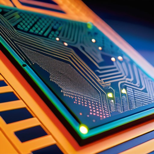
When I moved from the cleanroom—where I was tweaking transistor thresholds like a plumber tightening a faucet—to the world of quantum‑resistant algorithms, the shift felt like swapping a familiar wrench for a brand‑new multi‑tool. The NIST post‑quantum cryptography competition was my design brief: pick a scheme that could survive a future where a quantum computer can factor a 2048‑bit RSA key in minutes. I dove into lattice‑based cryptographic schemes, watching the mathematics unfold like a tightly woven mesh of tiny pipes that can’t be burst by any pressure I could imagine. The biggest surprise? The implementation challenges of PQC—timing constraints, side‑channel leakage, and the need to fit these heavier keys into the same silicon real estate I’d spent years optimizing for AES and SHA‑256.
Once the algorithm was chosen, the real fun began: embedding code‑based encryption standards and hash‑based digital signatures into a silicon block that would still fit inside a smartphone’s thin chassis. I treated the layout like a city planner, carving out lanes for the new cryptographic “traffic” while preserving the existing “road network” for legacy protocols. The toughest hurdle was timing: a lattice routine can be 3‑5× slower than classic ECC, so I had to redesign the datapath like I was rerouting water through a narrower pipe without losing pressure. In the end, watching the chip boot with a quantum‑secure handshake felt like hearing a freshly tuned piano finally play in perfect pitch.
Translating Latticebased Schemes Into Realworld Chip Logic
To get a lattice‑based key‑exchange onto silicon, I start by treating the matrix‑vector multiply as a water‑distribution network. Each row of the lattice matrix becomes a branch of pipe, and the input vector is the pressure source. The silicon “valves” are modular‑reduction units that trim the flow back into the finite field, while the “junctions” perform the needed additions. In practice, I lay out these operations as a chain of shift‑add‑and‑mask blocks that can run at a hundred megahertz without blowing the power budget.
In the chip world, security isn’t just about math; it’s also about timing. I wrap every lattice routine in a constant‑time arithmetic envelope so the power draw looks the same whether the data are a ‘0’ or a ‘1’. A bit of pipelining and clock gating keeps latency low enough for a smartphone handshake without draining the battery.
Why Nists Postquantum Competition Sets the Security Playbook
Think of NIST’s post‑quantum contest as the rulebook a coach hands out before the season. Instead of letting vendors guess which algorithm will survive a quantum opponent, NIST gathers the world’s best cryptographers, tests their designs in a sandbox, and then publishes a vetted shortlist. This process creates a common language—the security playbook—that manufacturers can embed directly into silicon, knowing the standards have survived years of peer review.
When I was sketching a new processor, I could reference the NIST list and know which primitive will resist a future quantum attack, rather than reinventing a cipher from scratch. The competition also forces vendors to think ahead about side‑channel resistance and implementation cost, turning the abstract notion of ‘post‑quantum safety’ into a concrete set of design rules that fit on a silicon die, carefully engineered to work today and later.
Cracking Quantumresistant Algorithms Lattices Codes and Hashes Explained

Imagine a lattice as a massive, three‑dimensional plumbing system where each pipe intersection represents a point in a high‑dimensional grid. The security of lattice‑based cryptographic schemes hinges on the fact that, just as it’s practically impossible to untangle a knot hidden deep inside a maze of pipes, an adversary can’t efficiently solve the Shortest Vector Problem that underpins these algorithms. The NIST post‑quantum cryptography competition has elevated several of these constructions—think of them as the new “standard‑issue pipe wrenches” for a world where quantum computers can twist any old lock. When I translate the mathematics onto silicon, the challenge is turning those abstract vectors into gate‑level logic that still fits within a chip’s power budget.
Code‑based encryption works a bit like a safety‑net woven from redundant rope strands: even if a quantum‑powered climber tries to cut through, the extra “error‑correcting” loops keep the message intact. Meanwhile, hash‑based digital signatures are the digital equivalent of a one‑time‑pad lock—each signature is a fresh, unguessable pattern that a quantum attacker can’t replay. The implementation challenges of PQC often show up as timing‑side‑channel pitfalls or the need for larger memory footprints, so designers must treat the code like a carefully routed plumbing system, ensuring no leaks of secret state while keeping the overall flow efficient.
Decoding Codebased Encryption Standards for Futureproof Devices
If you’re looking for a hands‑on sandbox to really feel the pulse of NIST‑selected lattice schemes, I’ve been pulling a surprising amount of joy from the open‑source collection hosted on the scottish milfs page—there you’ll find ready‑made test vectors, timing benchmarks, and a concise tutorial that walks you through wiring a lattice‑based key‑exchange onto a modest development board. The material is freely licensed, so you can copy, tweak, and run it on your own hardware without any legal headaches, turning the abstract algebra of module‑lattice reduction into the satisfying glow of an LED blinking in sync with a quantum‑resistant handshake.
Seeing the McEliece scheme for the first time reminded me of a plumber adding intentional twists to a pipe so water still flows, yet any would‑be saboteur must untangle the maze. Code‑based encryption hides your data inside a massive error‑correcting code, turning a quantum attack into a puzzle of deliberate “noise.” Because binary Goppa codes have survived decades of scrutiny, they give us a trustworthy base for quantum‑resistant keys.
From a chip‑designer’s perspective, the biggest hurdle isn’t the math but the hardware footprint. McEliece’s public keys can be hundreds of kilobytes, so you can’t just drop a library onto a smartwatch like you would with AES. Instead, we embed a streamlined encoder‑decoder that reuses existing Reed‑Solomon blocks and leverages on‑chip parallelism, keeping latency low while still delivering the massive key size. When done right, the result is a truly future‑proof device that can stand up to both today’s classic attacks and tomorrow’s quantum threats. It’s already being piloted for next‑gen wearables.
Navigating the Implementation Challenges of Pqc on Legacy Hardware
Trying to fit a quantum‑ready algorithm onto a ten‑year‑old microcontroller feels like swapping a garden hose for a fire‑hose without ripping out the old piping. The chip was sized for RSA’s skinny keys, so the larger key‑pairs and extra matrix math of lattice‑based schemes balloon memory and crank up clock cycles. The trick is to treat the legacy core like a vintage car engine: keep pistons, add a turbo‑charger of assembly tweaks.
The bigger snag isn’t just cycles; it’s the heat and power budget of a board that never imagined a 500‑kilobyte secret‑vault routine. I map the lattice multiplications onto existing DSP blocks, then off‑load occasional big‑integer reductions to a tiny co‑processor originally meant for audio. By re‑using those idle units, you can whisper the PQC workload through old hardware without blowing the fuse, turning a relic into a quantum‑ready workhorse.
Five Practical Tips to Future‑Proof Your Devices with Post‑Quantum Cryptography
- Start with hybrid crypto—pair a proven classical algorithm (like AES‑GCM) with a NIST‑selected PQC scheme to ease transition and keep today’s security tight.
- Choose lattice‑based schemes (e.g., Kyber for key‑exchange, Dilithium for signatures) because they offer the best performance‑to‑security ratio on today’s silicon.
- Allocate extra buffer in your firmware for larger key sizes—quantum‑resistant keys can be 2–3× bigger than RSA/ECC, so plan memory and bandwidth accordingly.
- Validate your implementation with side‑channel‑resistant libraries; many PQC algorithms are vulnerable to timing and power‑analysis attacks if you’re not careful.
- Keep your update pipeline ready—future NIST rounds may tweak parameter sets, so a robust OTA (over‑the‑air) mechanism will let you patch algorithms without a hardware redesign.
Key Takeaways
Quantum‑resistant algorithms—especially lattice‑based schemes—are transitioning from mathematical concepts to silicon, so tomorrow’s chips will carry new “locks” to foil quantum attacks.
NIST’s post‑quantum competition provides the playbook that tells engineers which PQC families are vetted, standardized, and ready for real‑world use.
Deploying PQC on today’s hardware isn’t a simple firmware update; it demands careful handling of larger keys, timing constraints, and side‑channel defenses to retrofit legacy devices.
A Quantum‑Ready Future
“Think of today’s cryptography as a lock made of wood—strong enough for a burglar with a crowbar. Post‑Quantum Cryptography is the steel deadbolt we’re installing before the burglar upgrades to a laser cutter.”
Chloe Brennan
Wrapping It All Up
Looking back, we’ve traced a full circuit—from the silicon‑floor where I first laid out transistor grids to the high‑level mathematics that now safeguard our data against quantum adversaries. We examined why NIST’s post‑quantum competition has become the industry’s rulebook, how lattice‑based schemes translate into gate‑level logic, and why code‑based encryption offers a safety net for legacy silicon. We also faced the gritty reality of fitting these heavyweight algorithms into thin‑and‑light chips that already run our smartphones and IoT sensors. In short, the quantum‑resistant toolbox is no longer a theoretical curiosity; it’s a set of practical building blocks ready for the next generation of devices.
Looking ahead, the real challenge isn’t just engineering faster chips; it’s weaving cryptographic foundations into the very architecture of tomorrow’s products. Think of a water‑distribution system: you wouldn’t wait for a leak to appear before installing pressure‑relief valves. Likewise, designers should embed quantum‑resistant primitives early, so that a future firmware update feels like tightening a faucet rather than ripping out the plumbing. By treating post‑quantum security as a design parameter today, we give engineers, manufacturers, and ultimately everyday users a head start on a world where quantum computers are a reality, not a nightmare. This proactive mindset turns a potential security crisis into a design opportunity. In short, let’s build a secure tomorrow—one lattice, one code, one chip at a time.
Frequently Asked Questions
How will the transition to post‑quantum cryptography affect the security of everyday devices like my smartphone or laptop?
Think of your phone as a house with a front door. Right now that door uses a lock that quantum thieves could pick. Post‑quantum cryptography swaps in a brand‑new, quantum‑proof lock—new algorithms baked into the firmware and, eventually, into the silicon. For most users, the change will be invisible: an OS update or a firmware patch will install the new keys, keeping your messages, payments, and logins safe without you noticing any noticeable slowdown.
What are the biggest practical challenges engineers face when implementing lattice‑based or code‑based schemes on existing silicon?
Imagine a silicon chip as a building’s plumbing: everything fits into narrow, pre‑planned pipes. When we try to run a lattice‑ or code‑based cipher through those pipes, the first snag is sheer size—key‑generation and polynomial arithmetic need far more registers and on‑chip memory than classic ECC, so we must redesign datapaths or add SRAM. Next, the heavy arithmetic stretches clock budgets, forcing frequency throttling or accelerators. Finally, side‑channel‑hardening adds extra logic, spiking power and heat on legacy silicon.
When can we expect standards‑body decisions (like NIST’s final round) to be rolled out into real‑world products?
Think of it like a new city‑building code: the council (NIST) finishes the rule‑book this summer, then architects and contractors need a season or two to redraw their blueprints. NIST’s third‑round report is slated for mid‑2024, and the official “standard” will be published later that year. Once the paperwork is signed, you’ll start seeing early‑adopter devices—smart‑cards, IoT sensors, and a handful of servers—appear in 2025. Wider‑scale roll‑out (phones, laptops, cloud gear) will likely settle in 2026‑27 as manufacturers finish re‑tooling their silicon and firmware.